How to Fix a Mechanical Keyboard PCB: Soldering Guide

Fixing a broken mechanical keyboard PCB usually involves re-soldering a loose hotswap socket or bridging a damaged trace with a small piece of wire. With a basic soldering iron, some flux, and a multimeter, you can repair the most common keyboard hardware failures yourself rather than replacing the entire keyboard. Most repairs take 15–30 minutes once you’ve identified the fault.
ESD Safety First
Before touching any PCB, establish your ESD (electrostatic discharge) precautions. A static discharge too small to feel can permanently destroy the microcontroller or individual key matrix diodes on a keyboard PCB. Two steps cover the vast majority of builds:
- Anti-static wrist strap: A $5 wrist strap connected to an earth ground (the ground prong of a wall outlet, or a metal chassis connected to ground) keeps your body at the same potential as the board. Wear it whenever the PCB is out of the case.
- Work surface: An anti-static mat or even a sheet of aluminum foil connected to ground prevents static buildup from the workbench surface transferring to the PCB.
Avoid working on carpeted floors in dry environments - this is where most ESD damage happens. If you must work without a strap, ground yourself by touching a grounded metal object (a computer case plugged in but powered off) before touching the PCB, and avoid shuffling your feet.
Diagnosing the Problem Before You Solder
Accurate diagnosis saves time and prevents unnecessary desoldering. Work through software and hardware checks before applying heat.
Software Diagnosis via QMK/VIA
QMK keyboards are testable via the QMK Firmware matrix debug mode or through VIA without disassembly. Open VIA, navigate to the “Key Tester” tab, and press every key. Failed keys show up as non-responsive - but this tells you the switch position, not whether the fault is in the switch or the PCB.
The quick test to distinguish switch from PCB: remove the suspect switch and use metal tweezers to briefly short the two through-hole pads (or the two hotswap socket pads) where the switch sits. If the keypress registers in VIA, the PCB is fine and the switch is the problem. If shorting the pads produces no response, the PCB has a fault at that position.
Visual Inspection Under Magnification
Remove the PCB from the keyboard case and examine the problem area under a 10x loupe or illuminated magnifying glass. Common visible defects:
- Cold solder joints: dull, grey, or crystalline solder around a pad rather than shiny and smooth
- Lifted pads: the copper pad has separated from the PCB substrate - visible as a gap or slight elevation
- Cracked PCB traces: hairline cracks in the copper traces near flex stress points (common near screws and PCB cutouts)
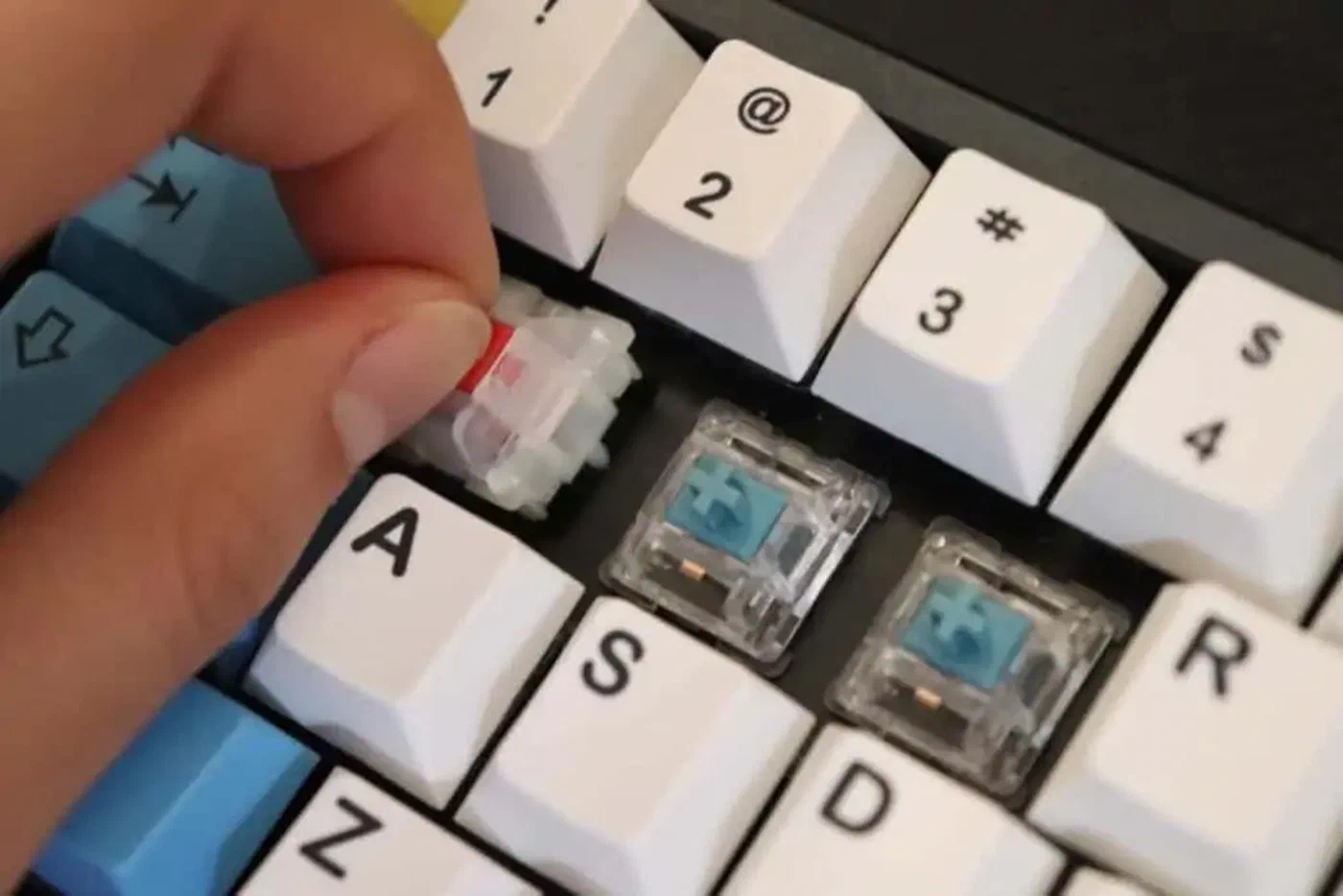
- Damaged hotswap sockets: the socket is visibly lifted, bent, or has lost one of its retaining pins
Multimeter Continuity Testing
A multimeter in continuity mode (the mode that beeps when the probes are connected) is essential for tracing broken connections. Set your multimeter to continuity mode, then:
- Touch both probes to the two pads of the suspect hotswap socket. You should get continuity between the pads and the switch’s travel path through the matrix.
- Trace from the suspect pad toward the MCU, testing continuity at each via and junction you can reach. Where continuity disappears, the fault is between your last good test point and the current one.
This systematic approach localizes trace breaks to specific PCB segments, telling you exactly where to apply conductive ink or a wire jumper.
Tools and Materials You Actually Need
Keyboard PCB repair does not require a professional electronics workstation, but investing in the right tools prevents further damage.
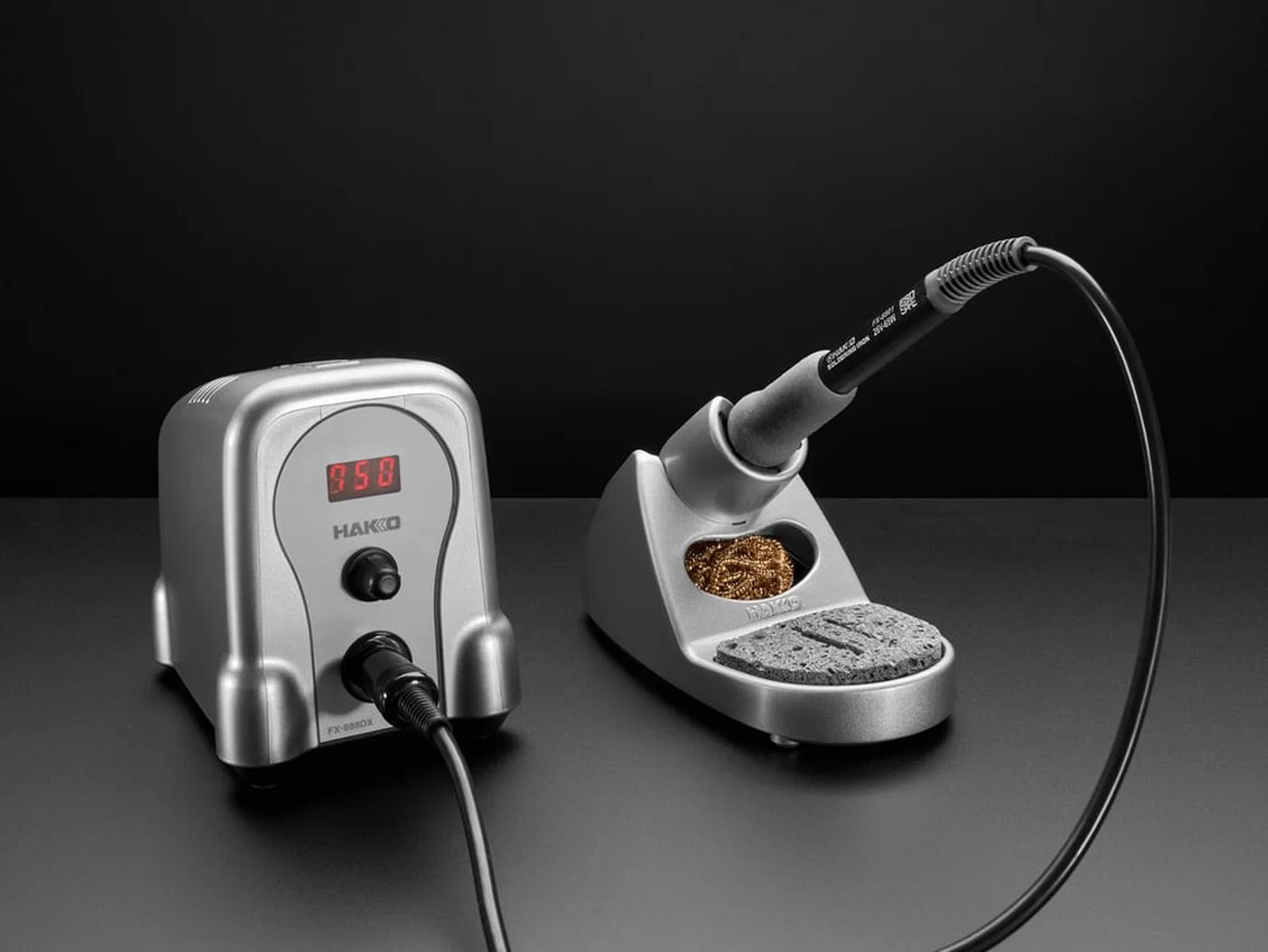
Soldering iron: A temperature-controlled station is strongly recommended. Fixed-temperature “pencil” irons commonly sold for $15–20 run too hot for delicate PCB work, risking lifted pads and burnt traces. The Hakko FX-888D ($110) and the TS101 portable iron ($40–50) are the two most popular choices in the keyboard community. Set temperature to 300–320°C for standard keyboard PCB work - high enough to melt solder quickly, low enough to avoid damage.
Solder: 60/40 or 63/37 rosin-core solder at 0.6mm diameter. Thinner diameter prevents bridging small hotswap pads and SMD component pads. Lead-free solder requires higher iron temperatures and doesn’t flow as smoothly - for hobby repair work, leaded solder produces noticeably better results at lower temperatures.
Flux: No-clean rosin flux pen is the single most useful addition to a keyboard repair kit. Flux dramatically improves solder flow, reduces the likelihood of cold joints, and makes re-flowing existing solder joints significantly easier. Apply it liberally before any solder work on a keyboard PCB.
Desoldering tools: For removing hotswap sockets or switches, desoldering braid (flux-coated copper wick) is the most controllable method - lay it over the pad, apply heat, and the solder wicks into the braid. A solder sucker (spring-loaded piston) is faster but requires more practice to avoid PCB damage.
Extras: Brass tip cleaner (not the sponge - brass wire doesn’t cool the tip), 99% isopropyl alcohol and cotton swabs for flux residue cleanup, and a PCB holder or third-hand tool to keep the board stable during work.
Re-Soldering a Loose Hotswap Socket
Loose or torn hotswap sockets are the most common mechanical keyboard PCB failure, particularly on boards that experience frequent switch swapping or mechanical stress. A loose socket produces intermittent actuation - the key works sometimes, fails to register other times, or only registers with specific finger pressure.
Identifying a loose socket: Gently wiggle the socket with tweezers. If it moves at all relative to the PCB, it’s loose. Also check if only one pin is registering - a socket with one good pad and one cold joint will show as working when the tweezer test is done carefully.
Safe removal: The key technique is applying flux to both pads first, then heating both pads simultaneously with the iron’s tip while gently lifting the socket. A socket heated on only one pad while you try to pry it off will tear the other pad - the most common way beginners damage PCBs.
1. Apply flux pen to both socket pads generously
2. Touch iron tip between the two pads at the base of the socket
3. Move tip to heat both simultaneously (requires some tip manipulation)
4. When solder melts on both, lift socket straight up with tweezers
Pad repair if lifted: If the copper pad peels up with the socket, you have two options. A copper pad repair kit ($10–15) provides adhesive-backed copper pads that you solder over the damaged area. For a single pad, a drop of conductive silver epoxy (Bare Conductive Electric Paint, or similar) applied carefully to the damaged trace can bridge the connection - it cures in 15 minutes and is solderable once cured.
Installing the new socket: Pre-tin the PCB pads (apply a small amount of fresh solder to each pad before placing the socket), position the new socket, then touch the iron briefly to each pad to reflow.
Repairing a Damaged PCB Trace
A broken trace - a hairline crack in the copper pathway between components - is more intimidating than a loose socket but entirely fixable with the right approach.
Locating the break: After continuity testing identifies the segment containing the fault, clean the area with IPA and examine closely under magnification. Trace breaks often appear at corners, near mounting holes (flex stress), or at the edges of PCB cutouts. The break may be invisible to the naked eye - very fine cracks in thin traces require a loupe.
Conductive silver ink pen repair: For breaks in short trace segments (under 10mm), a conductive silver ink pen is the cleanest repair method. Clean the area with IPA, let it dry completely, then trace over the broken segment with a steady hand. Apply two or three coats, allowing 10 minutes between each for curing. Test continuity after the final cure. Silver ink pens cost around $20 and handle most short trace repairs well.
Wire jumper method: For longer trace breaks or in areas where silver ink has poor adhesion, a wire jumper is more reliable. Use 30AWG wire-wrap wire - it’s thin enough to lie flat without creating a stress point. Strip both ends, tin them with solder, then solder one end at a known-good point on each side of the break. The wire jumps across the damaged section.
Insulating the repair: Any exposed copper should be covered after repair to prevent accidental shorts and oxidation. UV-cure solder mask (available in pen form) is ideal - apply, cure with a UV flashlight for 60 seconds, and the trace is protected. Clear nail polish is a functional substitute for hobby use.
Replacing a Failed MCU or Diode
These are more advanced repairs, but well within reach for anyone comfortable with SMD rework.
Diode replacement: Each key switch in a keyboard matrix has a series diode that prevents ghosting. Failed diodes are identified by continuity testing: a good diode passes current in one direction only; a failed diode passes in neither direction or both. Note the polarity before removal - the cathode band marking on the replacement must match the PCB silkscreen direction.
Diode removal with hot air: set the hot air station to 300–350°C, focus the nozzle on the diode, and apply gentle heat until the solder liquefies (5–10 seconds). Remove with tweezers. Place the new diode with the correct orientation, tack one end, confirm alignment, then solder the second end.
MCU replacement: This is the highest-complexity keyboard repair - generally only warranted if the keyboard has real sentimental or monetary value, since a replacement MCU plus the hot air rework work involved approaches the cost of a new entry-level board. ATmega32U4 and RP2040 are the two most common keyboard MCUs in 2026. Source replacements from Digi-Key or Mouser - avoid no-name clones for MCU replacements.
After MCU replacement, reflash the firmware using QMK Toolbox
. If the keyboard’s bootloader is the MCU’s native DFU bootloader, short the RESET and GROUND pads on the PCB (usually exposed test points) to force bootloader mode, then flash the appropriate .hex file.
When to give up: If the PCB has multiple lifted pads across several key positions, water damage with oxidized traces throughout, or a shattered PCB substrate, repair becomes impractical. The keyboard community on GeekHack , Reddit r/mechanicalkeyboards , and the keyboards.university resource site can help assess whether specific damage is worth pursuing.
Post-Repair Testing and Firmware Flashing
A complete post-repair validation prevents shipping yourself a keyboard that still has a subtle fault.
Full matrix test in VIA: Open the Key Tester, press every key including modifiers, media keys, and function row. Any key that fails to register requires investigation before reassembly.
QMK Toolbox firmware flash: If you replaced the MCU or suspect corrupted firmware, force bootloader mode and reflash the latest QMK firmware build for your keyboard. QMK’s firmware builder at config.qmk.fm generates firmware for hundreds of keyboards; the correct firmware file is usually documented in the keyboard’s QMK repository.
Electrical safety check: Before reconnecting to a computer, test with a multimeter that there’s no short between the USB VBUS pin and GND. A PCB short on VBUS can damage the host computer’s USB controller. Touch one probe to the USB connector’s pin 1 (VBUS, the wider pin on USB-A) and the other to GND. No continuity is the expected result - anything else requires investigation.
Stress test: After reassembly, type a 500-word document in a word processor or use a typing test site like keybr.com for 10 minutes. Intermittent faults that passed the static matrix test often reveal themselves under sustained typing that flexes the PCB slightly. If everything registers cleanly through 500+ keystrokes, your repair is solid.
The satisfaction of returning a dead keyboard to full functionality with a $0.50 socket and 20 minutes of work is considerable - and the skills transfer directly to any future PCB repair work on any embedded electronics project.